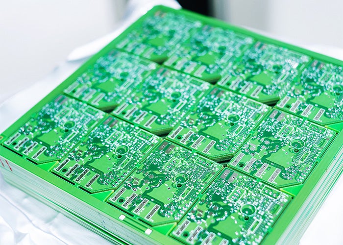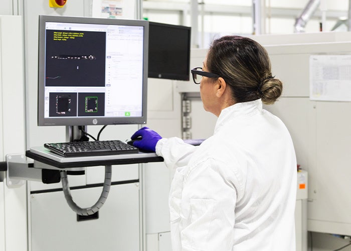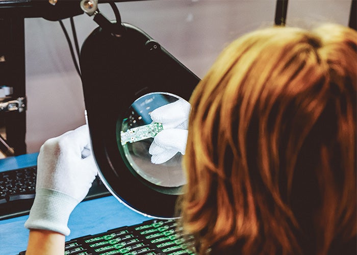
We have extensive experience assembling Large Form Factor boards of all sizes, including nonstandard large 91x91mm BGAs and 98x98mm CPU sockets. Our proprietary assembly process methodology helps prevent defects, such as HIP/NWO, resulting in faster new product introduction and a reliable manufacturing process.
Advanced printed circuit board assemblies (PCBAs) increasingly must perform more functions at a smaller size and weight. To meet your quality, performance, and speed targets, it’s critical to deploy the right advanced manufacturing and engineering technologies at the right stages.
Through our advanced testing, simulation, and miniaturization capabilities paired with our Design for Excellence services, we can help you determine key design improvements to optimize manufacturing before you ever begin production.
Our experience encompasses flip chip to the smallest passive and oddly-shaped components, high density assembly, low voiding soldering, proper underfill, edge bonding — including PCB protection with nano coating and conformal coating — and a deep understanding of materials impact on signal integrity. You can leverage our expertise to apply the latest technologies and techniques for flawless assembly and maximum performance.

Ensure PCBA manufacturing goes off without a hitch by first modeling systems in a virtual environment using finite element modeling.
We can analyze stresses and strains on the PCBA and simulate assembly process impact on solder joints, while conducting thermal analysis, to ensure that our assembly techniques and processes deliver the highest yield at the highest quality.

Even without a physical product, we can conduct thorough testing to assess the preparedness of your design. We’ll test your product virtually using pertinent data, then provide design feedback for increased reliability and efficient manufacturing. Once a product is manufactured, we can use signal and power integrity simulations to assist failure analysis and debug those assemblies.
When it comes time to assembly, lead with industry-leading capabilities — from large complex boards to 3D assembly and beyond.

Our knowledge of, and experience with, System-in-Package (SiP) means you get multiple electronic components in one integrated part to advance your miniaturization goals. And thanks to environmental technologies and additive processes, your electronic components can be more eco-friendly and support your circular economy efforts.
